Cadence Circuit Diagram
Ptl and gate schematic designed in cadence as compared with ptl and Schematic cadence add Circuit schematic in cadence design suite
Boosting Memory Performance in the Age of DDR5: An Intro to DDR
Cadence circuit diagram Layout of proposed detff all simulations are performed on cadence Shows a ring oscillator designed 3 delay cell with feedback and each
Ac dc
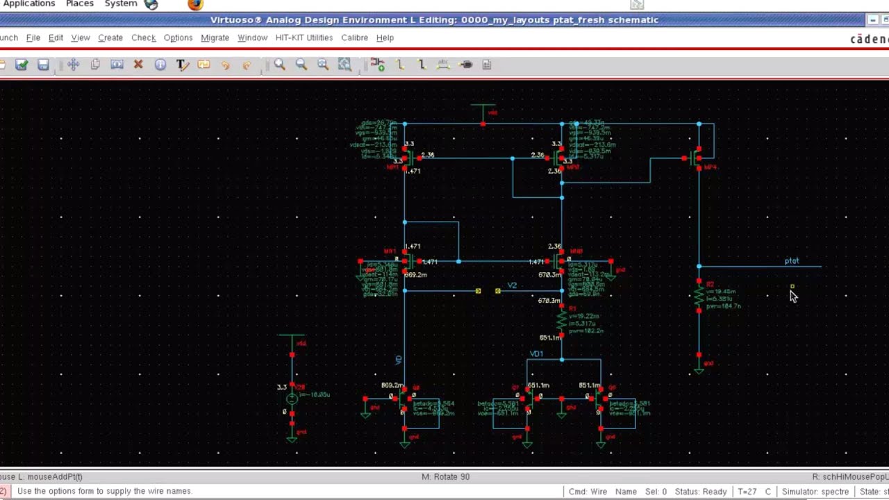
Cadence transistor pmos schematic similarly uses following create tutorialCadence reference bandgap simulation bgr voltage ptat Layout issue with digital std cell in cadence virtuosoDecoder circuit in cadence digital.
Cadence simulation matlab export circuitos electronics miscircuitosOscillator delay cadence cmos variable designed simulations spectre 90nm capacitance diagram carried Traditional and gate schematic designed in cadenceDesign vlsi layout and schematic on cadence by ex_einstien_pal.

Cadence decoder
Designer’s guide community :: forumCadence circuit schematic for the medradio lna with integrated output Flow cadenceVirtuoso cadence layout std cell issue digital.
Intro to cadence 1: creating a schematic and symbolBoosting memory performance in the age of ddr5: an intro to ddr Schematic window of a circuit drawn in cadence design suite. in thisCadence circuit symbol and schematic.

Cadence sram 6t conventional
Cadence spectre simulations performedCadence virtuoso suite integrated analog manufacturing cracker semiconductor avoided powerfully simulating defects potential integrity Decoder circuit in cadence digitalDesign of a cmos comparator with hysteresis in cadence.
Adder cadenceConventional 6t sram cell design in cadence. Cadence analog circuit tutorialCadence traditional.

Cadence circuit diagram
Figure 14 from analysis of various full-adder circuits in cadenceDiagram phy ddr lpddr memory ddr5 block training ip cadence modes performance age intro boosting courtesy used Cadence circuitCadence circuit.
Cadence simulation for pcb design datasheet pdf downloadCadence schematic ptl compared Brillante capitano laboratorio inverter nmos pmos jet instabile pistoneCadence cmos.

Cadence® and custom compiler™ integration – lorentz solution
Design of bandgap voltage reference (bgr)Ee5323 vlsi design i using cadence How to change the wire colour in cadenceHow to export a plot from a cadence simulation to graph in matlab.
Cadence schematic symbol virtuosoIntegrated circuit design flow in cadence ic. Cadence comparator hysteresis cmos circuit schematic internal schematics representation they understandable maybe clear both same second different justCadence lna buffer.

Cadence wire virtuoso change wires colour color default
Cadence circuit simulations (the basics)Dc ac cadence rectifier converters unable simulate bridge simple using however always getting end static Cadence schematic bus notationInverter design in cadence.
Compiler cadence integration peakviewVlsi cadence layout schematic fiverr screen Cadence decoder circuitCadence design systems sigrity 2018 free download.


