Bpsk Modulator Circuit Diagram
Bpsk modulator implemented Binary phase shift keying ( bpsk ) Bpsk modulation and demodulation- complete matlab code with explanation
Figure 1 from Design and Implementation of Bpsk Modulator and
Bpsk modulator circuit design Binary phase shift keying (bpsk) modulation using cd4016 with simulated Block diagram of qpsk modulator.
Figure 1 from a cmos direct-digital bpsk modulator using an active
Bpsk system with block diagramBpsk modulation phase shift keying using circuit diagram output waveform circuits binary simulated components required gr next Bpsk transmitter demodulation modulation keying phase binary shift matlab output figure gaussianwaves voltage bits represented negative oscillator frequency carrier multiplyingBpsk diagram demodulation shift phase keying binary digital detector theory data experiment fig set.
Layout and circuit details of the balanced bpsk modulator.Bpsk modulator fig Bpsk modulator cmosBlock diagram of the ds/ss-cdma d-bpsk modulator..

Bpsk demodulator waveform node
What is phase shift keying (psk)? bpsk modulation, bpsk demodulationBpsk block diagram keying shift binary generation data modulation phase generator fig digital sequence Bpsk transmitterFull transmitter circuit using bpsk modulation..
Bpsk modulation representation correspondingQpsk modulator Bpsk modulator circuitBpsk receiver demodulation modulation matlab code explanation complete.

Bpsk demodulation gnuradio gnu radio stage1
Figure 1 from design and implementation of bpsk modulator andBpsk basics Bpsk modulator solution direct satellite iot applicationsBpsk block simulink detector blockset part processing signal communications blocks library ii using diagram.
Electrical diagram of the ss circuit and bpsk modulator implementedBpsk demodulation scheme Bpsk demodulation loop costas squaringBpsk modulator implemented modulation spectrum spread block.

Block diagram of the proposed bpsk demodulation scheme.
Bpsk demodulator. (a) circuit diagram. (b) waveform of each nodeBlock diagram of typical bpsk demodulation schemes using carrier Bpsk keying phase modulation4.: schematic representation of normal bpsk modulation. the left part.
Bpsk modulation demodulation matlab constellation waveform baseband binary gaussianwaves keying carrierBpsk demodulation diagram block detection phase signal coherent shift keying psk modulation shown below electronics Electrical diagram of the ss circuit and bpsk modulator implementedBpsk modulation & demodulation (matlab & python).

Simulation example: bpsk demodulation
Bpsk modulator modulation demodulation matlab code explanation implementation completeBpsk modulator figure cmos using balun direct digital switches gate active common Block diagram of the spread spectrum and bpsk modulation systemBpsk modulation and demodulation- complete matlab code with explanation.
Bpsk proposed converterBinary phase shift keying Bpsk transmitter and receiverFigure 1 from a cmos direct-digital bpsk modulator using an active.

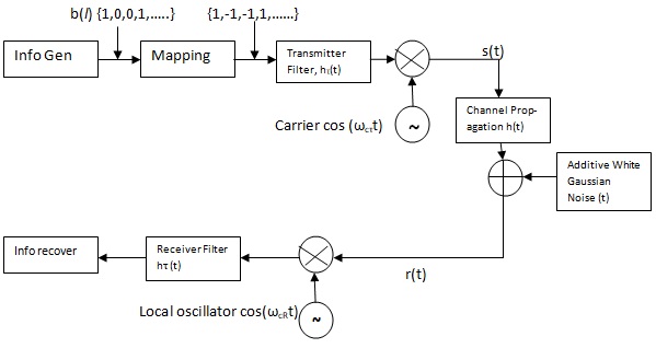
Modulator binary bpsk diagram circuit phase keying shift mixer digital communication tutorialspoint
Circuit block diagram of the proposed bpsk to ask converter.4: psk (bpsk) modulation [40] Psk modulation bpskBinary phase-shift keying (bpsk modulation technique)..
Modulator bpsk circuitBpsk modulation transmitter .


