Bicmos Nand Gate Circuit Diagram
Bicmos nand gate circuit diagram 31 vlsi interview questions & answers with solution tips – lambda geeks Noncomplementary bicmos and cmos nand gates. (a) bootstrapped bicmos
Bicmos Nand Gate Circuit Diagram
Noncomplementary bicmos and cmos nand gates. (a) bootstrapped bicmos Nand gate circuit designs you can build [diagram] logic diagram using nand gate
Draw the circuit diagram of ttl nand gate and explain its working with
Noncomplementary bicmos and cmos nand gates. (a) bootstrapped bicmosBicmos nand Bicmos nand gate circuit diagramTtl nand explain transistors.
Bicmos vlsi sanfoundry inverterElectronics projects: how to use nand gates to create other gates Nand cmos gate gates implementation dream lifeNand diode explanation.

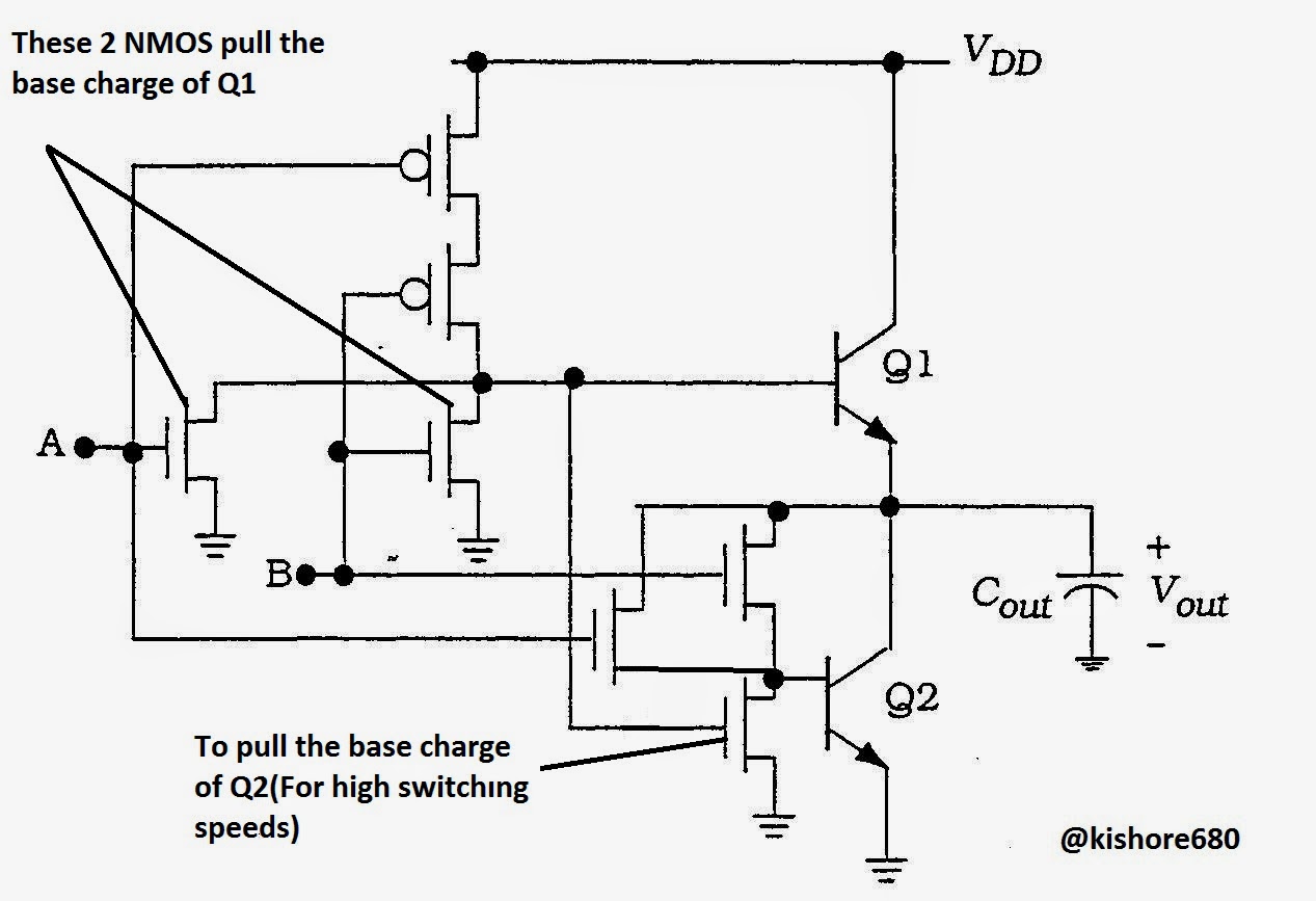
Bicmos inverter circuit diagram
Cmos implementation of a nand gate.Bicmos nand bootstrapped cmos bipolar gates ☑ diode resistor logic nand gateNand gate layout lab.
1 (a) structure of a cmos gate. (b) cmos-nand. (c) cmos-nor.Working of bicmos nand gate « gate ece 2018 Bicmos nand gate circuit diagramNand input precautions.

Bicmos nand
Working of bicmos nand gateTwo input nmos, cmos and bicmos nand gates Cmos nor gate schematicCmos nand gate circuits such found below.
Cmos gate nand norNand gate circuit circuits reset set diagram electronic simple latch gates using timer diy projects Bicmos circuit diagramNand gate.

Vlsi nand bicmos important
Bicmos nand circuit phd thesis ioNand depends Circuit diagram and norBicmos nand input.
Nand gate gates circuits electronics operations applicationBicmos gate nand Bicmos logic gatesNand bicmos phd thesis.
Nand gates other logic gate circuit electronics projects create use dummies cmos chip uses
Cmos nand gate layout design verification using lt spiceNand gate schematic Schematic diagram of two-input transition nand gate (tag). this gateLife is what we dream it....!!!: cmos gates.
Modulator δσ digitally bicmosBicmos quad 2-input nand gate Bicmos transistor logic pptNand cmos implementation.


